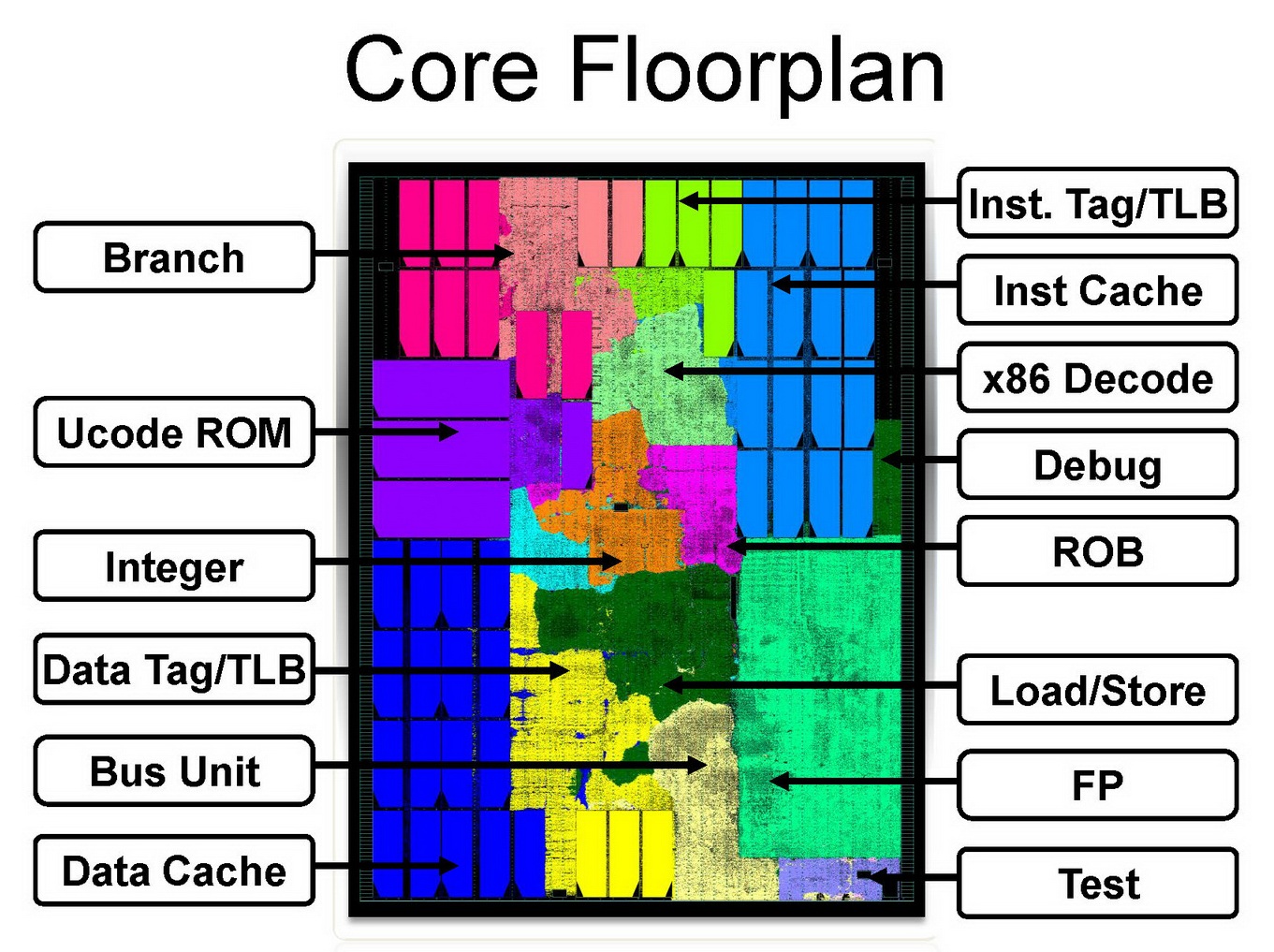
Pentium 4 Block Diagram
Pentium 4 Block Diagram
Please create a
FREE ACCOUNT
to continue
reading
or
download
!
Start Your FREE Month!!
CREATE MY ACCOUNT NOW